Pentium 3 Motherboard Schematic Diagram What Is Pentium Micr
Block diagram of our network processorto-pentium testbed. Adventures with a “working” pentium iii motherboard – linuxjedi's /dev/null Basic structure of a pentium microprocessor
PPT - Introduction to CMOS VLSI Design Lecture 22: Case Study: Intel
Intel pentium iii motherboard model d815eea2/d815epea2 25+ pentium 4 processor architecture block diagram Pentium p5 processor
Motherboard pentium s370
Lenovo w541 laptop mother board circuit diagramPentium motherboard How motherboards workWhat is pentium microprocessor? features and architecture of pentium.
Cpu microprocessor pentium processor registers microprocesadores processador componentes motherboard computadorCpu wiring diagram to motherboard skr e3 dip v1.1 32bit control board The pentium: an architectural history of the world’s most famousFunctional diagram of motherboard of pc.

Used 810 socket 370 motherboard + pentium 3 processor + 128mb sdram – 7
Schematic diagram ps3 motherboardLearn laptop motherboard schematic [circuit] diagram Yep! i bricked a pentium 3 motherboard (and how i fixed it) – linuxjediAsus motherboard circuit diagram.
Pentium processor worldMotherboard pentium cpu bidorbuy Schematic diagram of intel motherboard from mid-1990sHp desktop motherboard i810, intel pentium iii 1000 cpu 128 mb ram.

Motherboard connections connectors
File:computer motherboard to pentium iii 2003 000.jpgMotherboard circuit diagram download Pin by maurílio dias on 3d printer machinePentium microprocessors.
Motherboard & cpu bundlesPentium architecture iii micro ppt operations powerpoint presentation Pentium p5 processorMotherboard anatomy: connections and components of the pc motherboard.

Laptop schematic diagrams ~ digital world
Intel pentium 3 open motherboard with s+v+l (s370)Desktop motherboard schematic diagram pdf Shuttle fv24: the tiniest pentium iii motherboard. might make an itxStephanie seymour-david alaba: [get 33+] schematic diagram gigabyte.
Give me 5 marks answer in simple english pointwise explain pentiumPentium mainboard layout iii system basic microprocessors motherboard intel materials university Motherboard pentium shuttleDiagrama para laptop schematic tarjeta madre motherboard 2900 en images.

Pentium study case processors intel vlsi cmos instructions
.
.


Used 810 Socket 370 Motherboard + Pentium 3 Processor + 128MB SDRAM – 7

File:Computer motherboard to Pentium III 2003 000.JPG - Wikimedia Commons

Shuttle FV24: the tiniest Pentium III motherboard. Might make an ITX
![Stephanie Seymour-David Alaba: [Get 33+] Schematic Diagram Gigabyte](https://i.pinimg.com/originals/01/2c/b7/012cb7b8ebd993d90eef4e68ad4be99f.jpg)
Stephanie Seymour-David Alaba: [Get 33+] Schematic Diagram Gigabyte

Block Diagram of our Network Processorto-Pentium Testbed. | Download

PPT - Introduction to CMOS VLSI Design Lecture 22: Case Study: Intel
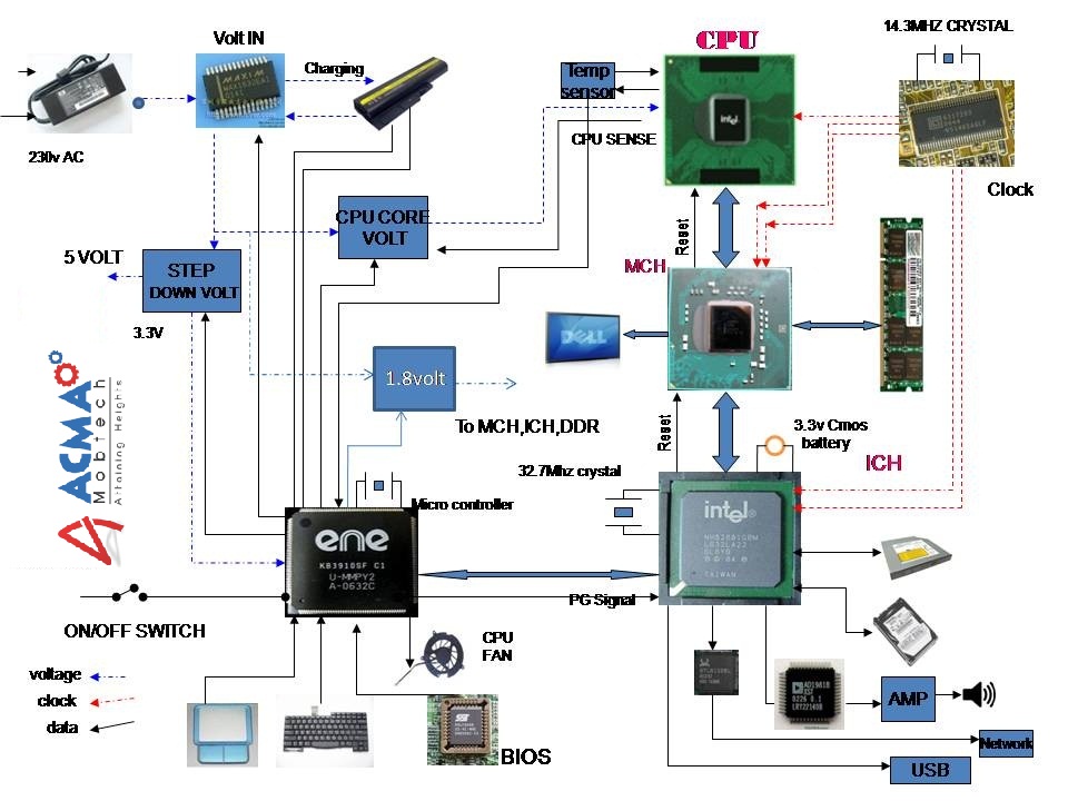
Laptop schematic diagrams ~ DIGITAL WORLD